CPU part 18 - One bus for everything else
With the caches, the CPU can read and write SDRAM, and it has its own internal registers. But the memory map has more: the ROM can also be read as data, the I/O region holds devices like UART, SPI, internal timers, and other interfaces and memories that do not require the lowest latency possible. In this post, all of those get connected via a single bus for everything that is not SDRAM.
Why not connect them all directly?
The obvious way to connect another memory is to put its output on the read path of MEM, next to the cache. A block RAM like the ROM gives its word one cycle after it gets the address, just like the cache, so a read from it would not even have to wait.
The problem is that this read path is one of the longest paths in the CPU. In a single cycle, the word comes out of the cache, the right memory is picked, the byte or halfword is taken out of it, and the result goes on to the register file and to the forwarding of the next instruction. Every memory that is added there makes the choice between memories a bit wider, and adds one more long wire from somewhere on the chip into the middle of the CPU. All the I/O devices and other memories would make the path have huge selection logic and long wires to the physical IO ports. And aside from this, it would make the CPU tightly coupled to I/O devices which might change independently of the CPU design, and make the overall design less modular.
The idea with the I/O devices (and the data access to the ROM) is that they do not need to be optimized for the lowest latency. They can tolerate a few extra cycles for the request to reach them and for the response to come back. This way, we can just put all the accesses to them over a single bus, and have a completely separate module handle the communication with the different types of I/O and memories. Having a bus almost always adds some latency in the form of communication overhead.
The bus
So everything outside SDRAM goes over one bus, with the same request and answer idea as in the post about waiting for memory. The CPU sends a request with the address, and for a write the data. Whatever is behind the bus does the read or write, and answers when it is done, with the word for a read. The CPU does not know or care what is behind it.
A read or write over the bus goes like this:
| Cycle in MEM | What happens |
|---|---|
| 1 | MEM sees that the instruction needs the bus, and is busy |
| 2 | the request goes out, from a register |
| 3 or later | the answer comes back, and the word goes into a register |
| next | MEM uses the word from that register, and the instruction moves on |
Two things in this table keep the bus away from the long paths of the CPU. The request is sent from a register, so the devices see a clean signal that does not depend on all the logic in front of it. And the word that comes back also goes into a register first, so the long wire from the device ends there, and not in the middle of the read path. Each of them costs a cycle, but for the devices behind the bus, that is acceptable.
To see how this impacts the pipeline, consider a program that reads a word from the ROM, writes it to the I/O region, and reads it back:
cycle               0   1   2   3   4   5   6   7   8   9   10  11  12  13
read 0 r1 r3        EX  MEM MEM MEM MEM WB
write 0 r2 r3       ID  EX  EX  EX  EX  MEM MEM MEM MEM WB
read 0 r2 r4        IF  ID  ID  ID  ID  EX  EX  EX  EX  MEM MEM MEM MEM WB
Each access spends four cycles in MEM, and everything behind it waits. Like before, a read or write is never flushed once it is in MEM, so every access makes exactly one request. That matters for many I/O devices: e.g. reading a byte from UART takes it out of the receive buffer, so the CPU must never read it twice, or for an instruction that should not have run.
Writes wait too
A write over the bus also waits for the answer. That gives a device the possibility to say “not yet”. For example, UART can only send one byte at a time, and if a program writes the next byte while the previous one is still being sent (which is the case if the UART controller returns early on a write, which it probably would), the UART can simply wait with its answer until it has room. The program does not have to check for that itself.
The rest of the reads
The CPU-internal registers and the unmapped addresses are not on the bus, as they are inside the CPU. But their reads now also take the slow path: the value goes into the same register first, and MEM uses it a cycle later. A read of a CPU-internal register is fine if it takes a few nanoseconds longer, and this way MEM chooses between only three words when it reads:
- the word from the cache
- the word that arrives from SDRAM at that moment, for early restart
- the word in the register of the slow path
GPU memory
There is one type of memory where I have not decided yet how I will connect it to the CPU: the GPU memories. The GPU has several block RAMs for its tile based rendering, and uses external SRAM for the bitmap framebuffer. Those tile based rendering memories are not that critical for performance as there are relatively few and do not need to be updated in a tight rendering loop (although I still have not written a complex NES-style tile-based game yet so I cannot say for sure), so I can probably connect those to the bus. However, the bitmap framebuffer is extremly performance critical as it is the bottleneck in software based rendering. In the previous FPGC version, I did connect the VRAM directly to the CPU’s internal data path, but I am currently considering forcing DMA for the framebuffer instead. That way, the CPU can just do the rendering in RAM using the L1d cache, trigger the DMA, and render the next frame while the copy is happening. Then, I could just connect it to the bus too for slower non-critical rendering where I do not want to use DMA.
What is behind the bus
In the simulation, a model sits behind the bus. Reads of the ROM come from the second port of the ROM (which is outside of the CPU), and the I/O and other regions are simple memories, so a program can read back what it wrote. The model also answers after a random number of cycles, to test that the CPU really waits for the answer properly.
On the first design to be physically tested, the first things behind the bus will be just the ROM and UART. The rest of the I/O devices, and at some point the GPU, come later.
Simulation
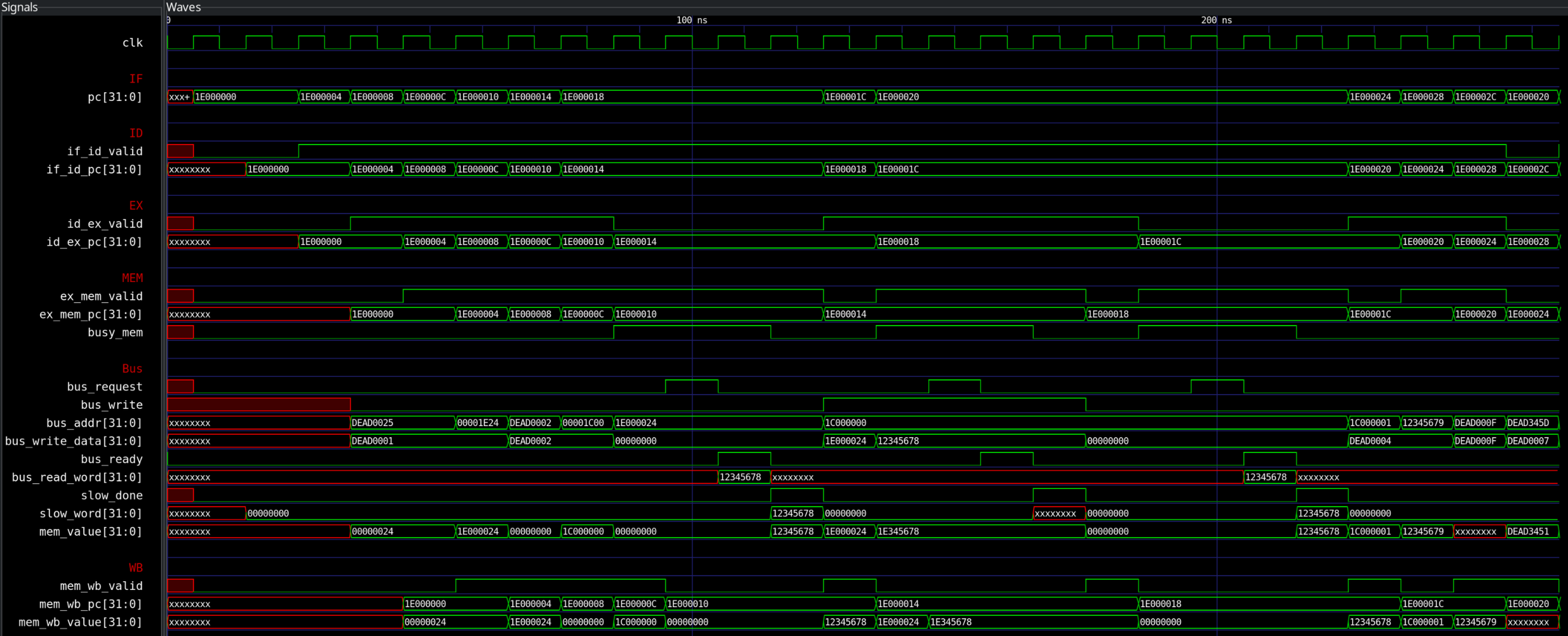
Here you can see the demo program from above.
- The read of the ROM enters MEM, and MEM is busy. In the next cycle the request goes out, with the address of the word in the ROM.
- One cycle later the answer comes, with the word. MEM is still busy for one more cycle, in which the word is in the register of the slow path, and then the read moves on to WB.
- The write and the second read do the same, with the address in the I/O region. The write sends its data with the request, and the second read gets that same word back.
Next steps
With this, the CPU itself is complete for now. The next big step is running it on the actual FPGA, with the ROM, SDRAM (which still needs the controller!), a simple UART, and a small program in the ROM to validate it works. For that, I first need an SDRAM controller for the cache controller to talk to, and a UART on the bus. Luckily, we are getting at a point where I can mostly copy designs from the previous FPGC version, as these components are quite modular and already tested by me in the past. Although, the SDRAM controller will need some modifications as the interface changed a bit from a 256 bit wide bus to an interative word-based bus.