CPU part 14 - L1 Cache part 1 (design + hits)
Waiting for memory is very expensive in a pipelined CPU: every cycle spent waiting throws away what pipelining gains. The FPGC uses SDRAM as main memory, which is fast in terms of bandwidth but slow in terms of latency. Caches are the solution to reduce latency. They are small, fast memories inside the CPU that keep a copy of the parts of SDRAM that are used the most. This post explains how caches work, what the options are, and how a cache hit works in the B32P4. Since caches (L1 cache in this case) are quite complex, there will be multiple posts about them with this being the first one.
Why caches work
SDRAM is cheap (although its price has hiked ~3x since the AI memory apocalypse) and large (tens of megabytes), but every initial access has to wait several cycles before the data comes out. The block RAMs inside the FPGA answer in one cycle, but these are typically in the order of kilobytes for most FPGAs unless you use a very expensive one.
A cache combines the two. It keeps copies of small pieces of SDRAM in block RAM, and as long as the CPU finds what it needs there (a hit), it never has to wait. This works because programs are quite predictable in what they use:
- Locality in time: what was used recently will probably be used again soon. Think of a loop, its counter and the variables it works on.
- Locality in space: what is next to something that was used will probably be used soon. Think of the next instruction, or the next element of an array.
Because of locality in space, caches copy small blocks of memory around them, called lines. When the CPU reads one word of a line, the rest of the line comes along, and the next instructions or array elements are then already there. This works because burst access on SDRAM makes reading lines more efficient than individual words.
Lines, index and tag
Each B32P4 cache has 128 lines of 32 bytes (8 words), so 4 KiB in total. Note that I might increase the cache size in the future depending on timing headroom and performance tests. The cache needs to know where each line belongs in SDRAM, so the address is split up into three parts:
address 0x0001234C:

bits   25 ........... 12   11 ..... 5   4 . 2   1 0
       00 0000 0001 0010   001 1010     011     00
tag = 0x12 index = 26 word 3 byte 0- The word and byte say where in the line the data is.
- The index says in which line of the cache it goes. With 128 lines, that is 7 bits.
- The tag is the rest of the address (SDRAM is 64 MiB on the FPGC, so only bits 25 to 0 matter). It is stored next to the line, so the cache knows which piece of SDRAM is in that line right now.
Next to each tag there is a valid bit, which says if the line holds anything at all, and, for the data cache, a dirty bit, which I will explain below. Reading the cache means reading the line at the index, and then checking if the stored tag is the same as the tag of the address, and if the valid bit is set. If so, it is a hit. Valid bits are needed because during initialization or reset the cache lines do not hold valid data yet.
Many addresses share the same index: 0x10000 and 0x11000 for example both go to line 0, with tags 0x10 and 0x11. Only one of them can be in the cache at a time, so a program that alternates between the two keeps throwing the other one out. That is called a conflict miss, and it is the main weakness of this kind of cache.
Where a line can go
The cache I now described is direct-mapped, meaning each address has exactly one line where it can go. There are other options that are more complex but should perform better.
| Option | Where a line can go | Pros | Cons | Used in |
|---|---|---|---|---|
| Direct-mapped | exactly one line, given by the index | simple and fast: one tag to compare, and the word comes straight out of the block RAM | conflict misses, when two often used addresses share an index | Some old CPUs around 1990 |
| N-way set-associative | one of N lines (the set), given by the index | far fewer conflict misses | N tags to compare, a multiplexer to pick the right line after the block RAM, and a rule for which line to replace | almost all modern CPUs: the L1 caches of current Intel and AMD CPUs are 8-way or more |
| Fully associative | any line | no conflict misses at all | every tag has to be compared at the same time, which only works for very small caches | small special caches, like the TLBs that translate virtual addresses |
With the previous FPGC design I started with a direct-mapped cache as it is the simplest to implement. I am keeping that because the L1 cache typically sat in the most timing critical path of the CPU.
Writing: write-through or write-back
Reading a cache only makes copies, but writing changes data, and then the copy in the cache and the original in SDRAM are no longer the same. There are two main ways to deal with that:
| Policy | How it works | Pros | Cons | Used in |
|---|---|---|---|---|
| Write-through | every write goes to the cache and to SDRAM | SDRAM is always up to date, and a line can be thrown out at any time | every write has to wait for SDRAM, unless a write buffer takes it over | the Intel 486, and still an option in many smaller CPUs |
| Write-back | a write only goes to the cache, and the line is marked as dirty. A dirty line is written to SDRAM when it is thrown out | writes are as fast as reads, and a variable that changes a lot is only written to SDRAM once | throwing out a dirty line takes extra time, and SDRAM can be out of date. | the data caches of almost every modern CPU |
And there is a second choice: what to do when a write misses.
- Write-allocate: first fetch the line into the cache, and then write it like a hit.
- No-write-allocate: write straight to SDRAM, and leave the cache alone.
Write-back almost always comes with write-allocate, and that is what the B32P4 does just like the previous FPGC version. A program writes most of its data more than once (the stack, local variables, an array it works on), so it makes sense to keep that data in the cache.
The one catch of write-back is that SDRAM can be out of date. For the CPU itself that does not matter, because it always looks in its cache first. But anything else that reads SDRAM directly, like a DMA transfer, could see old data. That is partially why the FPGC has instructions to write all dirty lines back to SDRAM.
What the FPGA offers in terms of RAM for the caches
The caches are made of the M9K block RAMs of the Cyclone IV. Each M9K holds 9 Kbit (1 KiB of data, plus a spare bit per byte), and the EP4CE40 that the FPGC uses has 126 of them. An M9K can be shaped as 8192 × 1 bit, 1024 × 9 bits, 512 × 18 bits or 256 × 36 bits, and has two ports, each of which can read or write at its own address. Like all block RAMs it gives its data one clock edge after it gets the address.
Each cache in the B32P4 consists of two arrays:
- A data array of 1024 words of 32 bits: 4 M9Ks. For the data cache, it is split into 4 byte lanes, so a write of a single byte only changes that byte.
- A tag array of 128 entries with the valid bit, the dirty bit and the tag: 1 M9K.
One of the new things in B32P4 is this split. A read gives exactly the one word it needs, together with the tag of its line. Previous FPGC versions kept a whole line in one wide block RAM word, which means a multiplexer has to pick out the right word afterwards, and that multiplexer would sit right on the critical path from the cache to the rest of the CPU.
Both caches together use 10 of the 126 M9Ks. The number of lines is configurable as a Verilog parameter, so if I want to increase the cache size later I could do this hopefully more easily without recomputing all the bits and addresses.
A hit in IF
The instruction cache (L1i) acts similar to the ROM (which is also just a piece of block RAM) during a cache hit. Both get the same fetch address at the same clock edge, so in the next cycle IF has both a ROM word and an L1i word with its tag. If the PC is in the ROM, IF takes the ROM word. Otherwise it checks the tag, and on a hit takes the L1i word. Code is allowed to only run from ROM or SDRAM, so this should be fine.
A hit in the L1i is exactly as fast as reading from ROM: an instruction every cycle and the same cost for a jump, because the jump target is read from the cache at the same edge where it would be read from the ROM.
A hit in MEM
The data cache (L1d) gets its address from the address adder in EX, at the edge where the read or write moves into MEM, so in MEM the word and the tag are there right away.
- A read hit passes the word on through the read alignment, just like before. It costs no extra cycle. Only an instruction that needs the value right away waits a cycle, just like for every read.
- A write hit writes its bytes at the end of MEM, and at the same moment sets the dirty bit of its line by writing the tag entry again.
The write-then-access stall from the memory post stays: a read or write right behind a write waits one cycle in EX, because the write uses the address port of the cache in its cycle in MEM. Nothing else changes:
cycle               0   1   2   3   4   5   6   7
write 0 r13 r1      IF  ID  EX  MEM WB              hit: writes and sets the dirty bit
add r1 r2 r3            IF  ID  EX  MEM WB          no stall
read 4 r13 r4               IF  ID  EX  MEM WB      no stall: the write is in WB by then
read 8 r13 r5                   IF  ID  EX  MEM WB  no stall
One of the new things in B32P4 is that hits are handled in the pipeline itself. In the previous FPGC version, a hit in the data cache took a few cycles, and every write hit went through the cache controller. Now the cache controller only deals with misses, which makes it much smaller. I will go into more detail about this in the next post. Given the variable management I saw in the assembly output of the C compiler for the previous FPGC version, I have high hopes that this will cause a huge performance boost!
Simulation
Let’s look at the data cache arrays in a simulation.
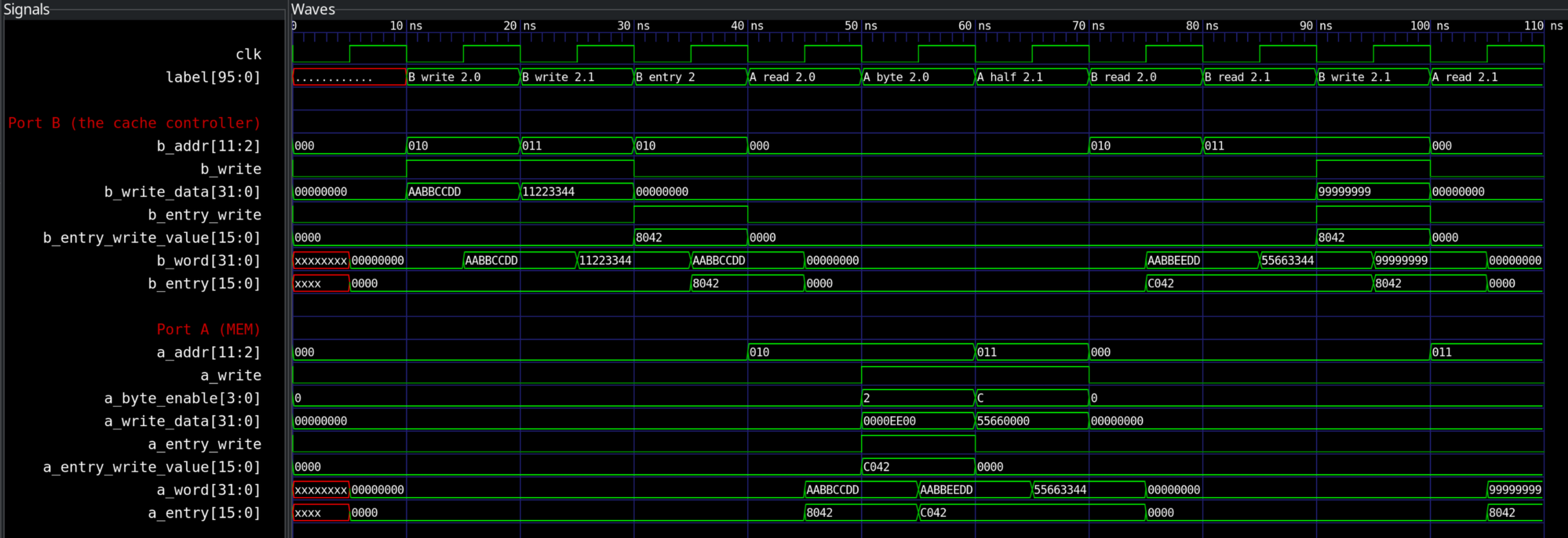
Here you can see the data and tag arrays of the L1d, with their two ports. Port B is the one the cache controller will use, and port A is the one MEM uses. Each port gives its word one clock edge after it gets its address.
- Port B fills two words of line 2 (
AABBCCDDand11223344), and writes the entry of line 2: valid, not dirty, tag0x42. - Port A reads word 0 of line 2 and its entry, as a read hit in MEM would.
- Port A writes one byte (
EEin the second lane), and writes the entry again with the dirty bit set, as a write hit does. Then it writes a halfword (5566in the upper two lanes) to word 1. A port that writes also reads what it wrote, so the new word shows up right away. - Port B reads both words back, as the cache controller does when it writes a dirty line back to SDRAM:
AABBEEDDand55663344. - At the end, port B writes a new word and a clean entry, and port A reads the new word.
Next steps
With hits, the CPU runs at full speed as long as the caches have what it needs. The next post is about the other case: what happens on a miss, how a dirty line goes back to SDRAM, and how the cache controller fits in.