CPU part 3 - Instruction decoder
The next component of the CPU to discuss is the instruction decoder. Where the ALU does the actual work, the decoder is the part that figures out what work needs to be done. It takes the 32-bit instruction word that was just fetched from memory, and turns it into the signals that tell the rest of the pipeline what to do with it.
What the decoder does
The decoder lives in the ID (instruction decode) stage. Its input is a single 32-bit instruction word, and its outputs are a bunch of signals that the other stages need: which registers to read, which register to write, what constant to use, what the ALU should do, whether the instruction reads or writes memory, and so on. Like the ALU, it is purely combinational logic without a clock: the outputs follow directly from the input. In contrast to the ALU, the logic here is extremely simple to implement in hardware, as it is mostly just extracting subfields from the instruction word.
To understand what the decoder has to do, we need to look at how an instruction is encoded. Every B32P4 instruction is one 32-bit word, with the opcode in the leftmost 4 bits. The opcode tells which type of instruction it is, and that determines what the other 28 bits mean. A few examples from the instruction set page:
         |31|30|29|28|27|26|25|24|23|22|21|20|19|18|17|16|15|14|13|12|11|10|09|08|07|06|05|04|03|02|01|00|
----------------------------------------------------------------------------------------------------------
 READ      1  1  1  0||----------------16 BIT CONSTANT---------------||--A REG---||-RD SUBOP-||--D REG---|
 BRANCH    0  1  1  0||----------------16 BIT CONSTANT---------------||--A REG---||--B REG---||-OPCODE||S|
 ARITHC    0  0  0  1||--OPCODE--||----------------16 BIT CONSTANT---------------||--A REG---||--D REG---|
 ARITH     0  0  0  0||--OPCODE--| x  x  x  x  x  x  x  x  x  x  x  x |--A REG---||--B REG---||--D REG---|
Something that I designed into the instruction set early on, and which makes the decoder a lot simpler, is that the fields are mostly at the same position in every instruction. The A register is (almost always) in bits [11:8], the B register in bits [7:4] and the D (destination) register in bits [3:0]. There are some exceptions though, but generally a lot of arguments are consistent between instructions.
Design choices
Register count
While techically more part of the instruction set design as described in my first CPU post, the instruction decoder really shows well why the FPGC has 16 registers instead of 32 or more. The entire ISA is a big puzzle where you have to define certain fields, and everythings needs to fit in 32 bits. With 16 registers, you only need 4 bits to encode a register number. By having 32 registers, which would allow you to write more efficient software as register access is faster than memory access, you would need 3 extra bits for instructions with an areg, breg and dreg. This in turn requires you to compromise on other fields like the constants or opcode. While you could design around this, you will probably end up with less alignment between instructions, which complicate the instruction decoder design. I could have gone quite different here, but ended up with the current design because it is good enough for me, although more optimal designs are certainly possible.
Register numbers are always passed on
The decoder outputs the register numbers areg, breg and dreg for every instruction, even when the instruction does not use them. This sounds a bit wasteful if you have a software background, but in hardware design this makes sense. The register file is read in the same stage as the decoding, and reading the register file takes time. If the register numbers first had to go through logic that checks whether the instruction actually uses them, the register file would have to wait for that logic, and the ID stage would get slower and contain more logic. Reading a register that is not needed is harmless as the value is simply ignored later.
Constant
Many instructions contain a constant, but in different places and with different sizes: 16 bits at two different positions (I could not get this perfectly aligned in my ISA), or 27 bits for jump. The decoder picks the right field and extends it to 32 bits, so the rest of the pipeline only ever sees one 32-bit constant.
Extending a number to more bits is less trivial than it sounds. For an unsigned number, you just add zeros on the left (zero-extension). For a signed number in two’s complement, you have to copy the sign bit instead (sign-extension), otherwise -5 (0xFFFB in 16 bits) would become 65531 instead of 0xFFFFFFFB. Most constants are sign-extended, so you can write add r1 -5 r3 or branch backward. The exceptions are load and loadhi, which are zero-extended, because they are used to build 32-bit values from two 16-bit halves.
There are a few nice tricks hidden in the constant, which reuse existing hardware instead of adding new logic:
savpc(save the program counter to a register) is decoded as the ALU’sloadoperation, with the PC as constant. So the ALU does not need an extra input for the PC.haltis a jump to itself, which is a relative jump with constant 0.ccache(clear the cache) is a relative jump with constant 4: a jump to the next instruction. This makes sure that every instruction after it is fetched again after the cache was cleared.
To make this possible, the decoder has two flags: const_add_pc when the constant needs the PC added to it (for savpc and jumpro), and jump_absolute for the jump instruction, where the constant is the target address itself instead of an offset from the PC. The decoder does not know the PC, so the actual adding happens in the rest of the ID stage.
One signal per instruction type
The most important output is the instruction type. Instead of passing the 4-bit opcode on through the pipeline and having each stage decode it again, the decoder outputs one signal per type of instruction: arith, mult, div, read, write, push, pop, branch, jump, jumpr, halt, reti, ccache and intid. Exactly one of them is 1 for every instruction (this is called one-hot).
This has two advantages. First, the decoder is the only module in the CPU that knows the opcodes and instruction formats. The rest of the CPU only sees named signals: the memory stage just checks write, and does not need to know that a write is opcode 1101. Creating these named signal early on prevents later stages to read the full instruction again and instead just requires them to read single bits/flags.
The types do not map one-to-one to opcodes: arith covers ARITH, ARITHC and savpc (all use the single-cycle ALU), and ARITHM is split into mult and div, because the multiplier and the divider are completely different units. This is a bit of a mismatch that can be confusing, but I do not see how I could have done this differently.
Illegal instructions do nothing
Not every possible instruction word is a valid instruction. Some ALU operations, branch conditions and read/write sizes are reserved. For those, the decoder sets illegal, and every other output (except the raw register numbers and fields) is 0. Since none of the instruction types is set, the instruction does nothing at all as it flows through the pipeline, so it automatically acts as a NOP without any special handling anywhere else. The illegal signal is only used to set a flag in the new error register, so that I can find out later that something went wrong.
Simulation
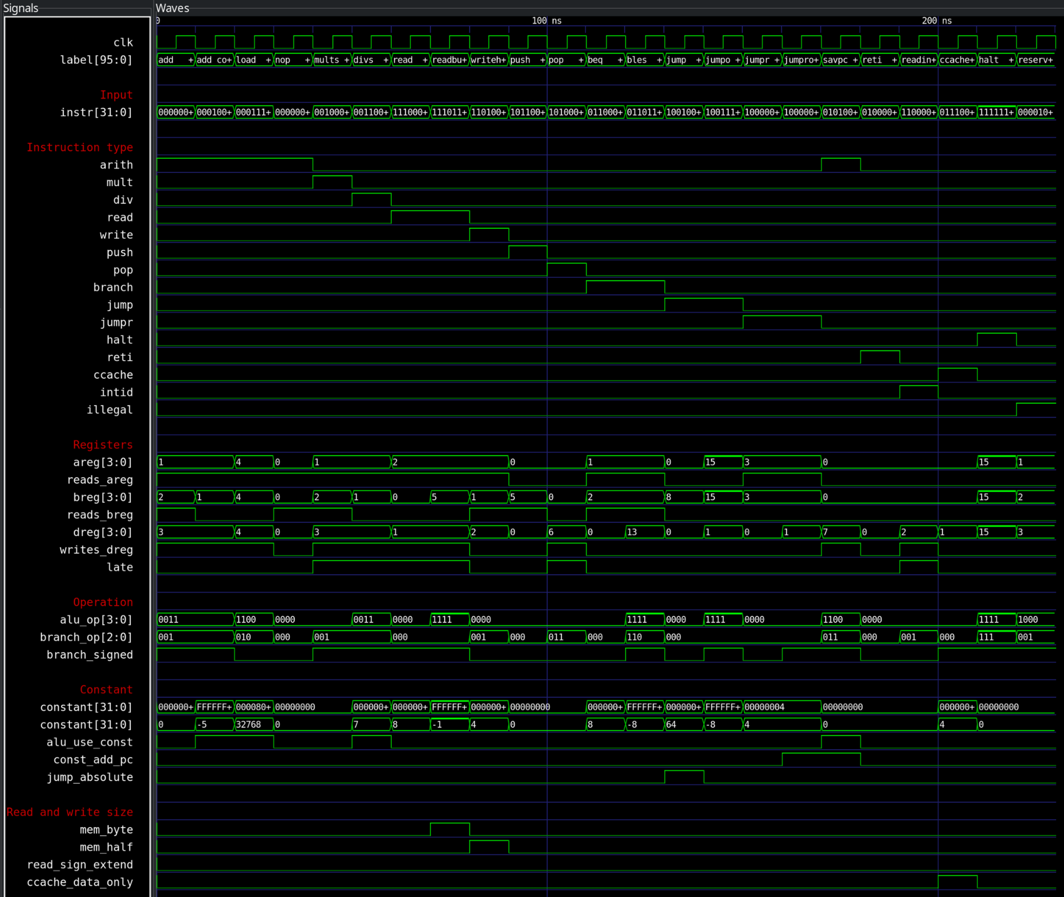
Here you can see the simulation of the instruction decoder in GTKWave. Only the instr field is the input, and all other signals are generated based on this input. Again, because this is combinational logic, the outputs change immediately in response to changes in the input instruction word, and the clk signal is just for spacing here.
Next steps
With the instruction decoded, the next step will be the register file, which uses the decoded register numbers and will be the first piece of synchronous logic.