CPU part 9 - Reading and writing memory
So far, the CPU could only work with its 16 registers. In this post we will make a start on actually reading from and writing to memory regions.
The memory map
The CPU has a 32-bit address space, which is divided into regions. Each region is a different memory or device. This memory map is what I ended up with in the previous FPGC design, and for now I am keeping it as-is (it might be changed later on). Note that almost all of these regions are still unused in the current CPU design and will be implemented later.
| Region | Start address | Size |
|---|---|---|
| SDRAM | 0x00000000 | 64 MiB |
| I/O | 0x1C000000 | 32 MiB |
| ROM | 0x1E000000 | 4 KiB |
| VRAM32 | 0x1E400000 | 4224 bytes |
| VRAM8 | 0x1E800000 | 32776 bytes |
| VRAMPX | 0x1EC00000 | 128 KiB |
| Palette | 0x1EC80000 | 1 KiB |
| CPU-internal I/O | 0x1F000000 | 16 bytes |
SDRAM holds the programs and their data, the I/O region contains I/O devices like UART and the SPI controllers, the ROM holds the bootloader, and the other regions are for the GPU that will be covered later. The CPU-internal I/O consists of a few registers inside the CPU itself, wich was one of the last things I added in the previous FPGC design to enable some cool features in the CPU (which will also come later). Everything in between is unmapped: reading there gives 0, and writing there does nothing. The current full memory map is on the instruction set documentation page.
For every read or write, the memory map unit checks in which region the address is, and gives one bit per region. This is the only part of the CPU that knows where the regions are.
No subtraction needed
If you write to 0x1E400004, that is address 4 inside VRAM32. You might think that the CPU has to subtract the start address of the region to get there, but it does not. When I designed this memory map, I made sure that every region starts at a multiple of a power of two that is at least as large as the region itself, which was really easy to do given the low amount of memory compared to the address width. This means that the low bits of the start address are all 0, and the low bits of any address in the region are already the position inside it:
0x1E400004 = 0001 1110 0100 0000 0000 0000 0000 0100
                                    └─ bits 12 to 0: 0x0004 ─┘
VRAM32 is less than 8 KiB, so the position inside it fits in the lowest 13 bits. And because VRAM32 starts at a multiple of 8 KiB, these 13 bits of its start address are all 0. So the memory can just take the bits it needs, and ignore the rest:
| Region | Start address | Word number from bits |
|---|---|---|
| SDRAM | 0x00000000 | 25 to 2 |
| ROM | 0x1E000000 | 11 to 2 |
| VRAM32 | 0x1E400000 | 12 to 2 |
| VRAM8 | 0x1E800000 | 15 to 2 |
| palette | 0x1EC80000 | 9 to 2 |
The lowest two bits are left out, because each memory holds 32-bit words: they tell which byte inside the word is meant, which we will need below. Selecting bits is just wiring, so it costs no logic at all.
There is one catch: some regions, like VRAM32 with its 1056 words, are not a power of two in size. The bits 12 to 2 can count up to 2047, so an address just after the end of VRAM32 would end up in a memory location that does not exist. That is why the memory map unit does check the exact end of every region, and treats everything after it as unmapped.
Bytes, halfwords and words
Memory is organised in 32-bit words, but a read or write can also be a byte (8 bits) or a halfword (16 bits, sometimes called a “short”). The lowest two bits of the address tell where in the word it is. FPGC is little-endian, so byte 0 is the lowest 8 bits of the word.
For a read, the memory gives the whole word, and the read alignment unit takes out the part that is needed. A byte or halfword is then extended to 32 bits, either with zeros (the unsigned reads ending in a u) or with copies of its highest bit, so that a negative number stays negative. With the word 0xAABBCCDD in memory:
| Instruction | Takes | Result |
|---|---|---|
read 0 | the whole word | 0xAABBCCDD |
readbu 0 | byte 0 | 0x000000DD |
readb 0 | byte 0 | 0xFFFFFFDD |
readbu 3 | byte 3 | 0x000000AA |
readhu 2 | bytes 2 and 3 | 0x0000AABB |
readh 2 | bytes 2 and 3 | 0xFFFFAABB |
A write works the other way around: the write alignment unit moves the byte or halfword to its place in the word, and tells the memory which bytes to write with four byte enables, one per byte. The other bytes in memory keep their value. With 0x11223344 in the register:
| Instruction | Data to memory | Byte enables |
|---|---|---|
write 0 | 0x11223344 | 1111 |
writeb 0 | 0x00000044 | 0001 |
writeb 2 | 0x00440000 | 0100 |
writeh 2 | 0x33440000 | 1100 |
A halfword should be at an even address, and a word at a multiple of 4. If it is not, the address is rounded down: a readh at offset 1 reads bytes 0 and 1. Such an access most likely is a bug in the program, so in the in the future I should make sure this is reported in the to-be-implemented error register.
Note that until the last version of the previous FPGC design, the entire CPU was word-addressable instead of byte-addressable, meaning that you had to read/write an entire 32-bit word at a time, and the lowest two bits of the address were ignored. This simplifies the design a lot, but comes at the cost of inefficiency of writing byte data like text (which did not matter because 64MiB is huge) and also makes porting existing software more difficult (which was ultimately the reason for changing it).
Reads and writes in the pipeline
The address of a read or write is computed in EX by the address adder, which I introduced in the branch post. As explained in the register file post, a block RAM needs its address one clock edge before it gives the data. So the address goes straight from the adder into the memory, at the end of EX, and the word comes out during MEM. That way, a read takes just one cycle in MEM, like every other instruction. One of the new things in B32P4 is that this will also go for the data cache: a read that finds its data in the cache never has to wait either.
A write uses the same address adder, but it writes the memory at the end of MEM, when the write commits. Before that, it could still be flushed by a branch in front of it, so it should not change anything yet.
The value of a read only exists at the end of MEM, so it is a late result. The late-result stall from the forwarding post now finally has something to do: an instruction that needs the value right away waits one cycle in ID.
The write-then-access stall
The memory has only one address input. A read in EX uses it to give its address, while a write in MEM uses it to write at its own address. When both happen in the same cycle, one of them has to wait. The write goes first, as it is the older instruction and already in MEM, so the read waits one cycle in EX. This is the write-then-access stall. example:
cycle            0   1   2   3   4   5   6   7
write 0 r1 r2    IF  ID  EX  MEM WB
read 0 r1 r3         IF  ID  EX  EX  MEM WB
readb 0 r1 r4            IF  ID  ID  EX  MEM WB
In cycle 3, the write writes the memory, and the read gives its address one cycle later. Because of this, the read sees the value that was just written, even though it reads the same address right after the write. So the stall does two things at once: it shares the address input, and it keeps reads and writes in the right order. A write directly behind a write also waits, which will be needed once the data cache is added, as a write then also has to check the cache in EX.
This costs a cycle, but only when a write is directly followed by another read or write, which is not very common in compiled code.
This is also the first time EX can stall while MEM and WB move on. So it is also the first time the “a stalled EX keeps its values” rule from the forwarding post is needed: when the stalled read got its address register forwarded from WB, that value would otherwise be gone a cycle later.
An ideal memory for now
For now, the only memory behind all of this is a block RAM that stands in for the SDRAM. It always answers in one cycle, which is exactly how the data cache will behave when it has the data. The real SDRAM can take many cycles, which comes with the cache, and the ROM and video memories are added later too. Until then, reading from any other region gives 0.
Simulation
Let’s go over the new modules plus the MEM stage in GTKWave.
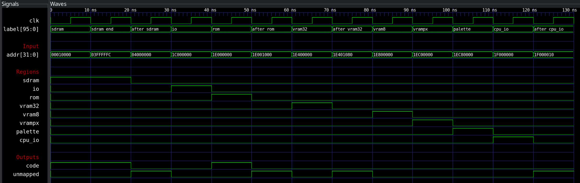
Here you can see the memory map unit, with one address in every region, and also the first address after the end of some of them. Like the other two units we just made, this is combinational logic, so the clk signal is just for spacing.
- Every address in a region sets exactly one region bit, and
codeis set for SDRAM and ROM, the only regions a program can run from. - after vram32 (
0x1E401080) is the first address after the 1056 words of VRAM32. Its bits 12 to 2 point just past the last word of VRAM32’s memory, so it is unmapped.
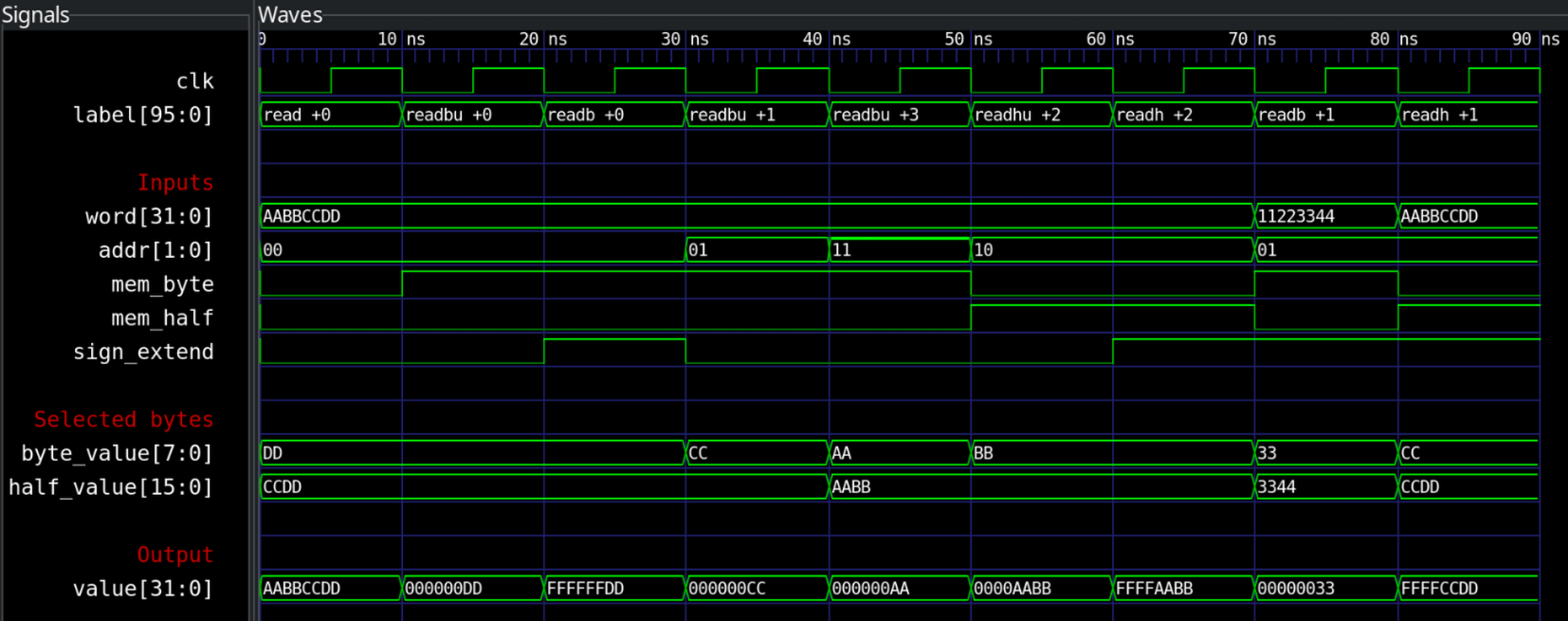
Here you can see the read alignment unit, with the reads from the table above, plus a few more.
byte_valueandhalf_valueare the byte and halfword at the address, before they are extended.- readb +0 and readbu +0 take the same byte, but only the signed read fills the upper bits with ones.
- The last case is a
readhat offset 1, which is rounded down, so it reads the same halfword as offset 0.
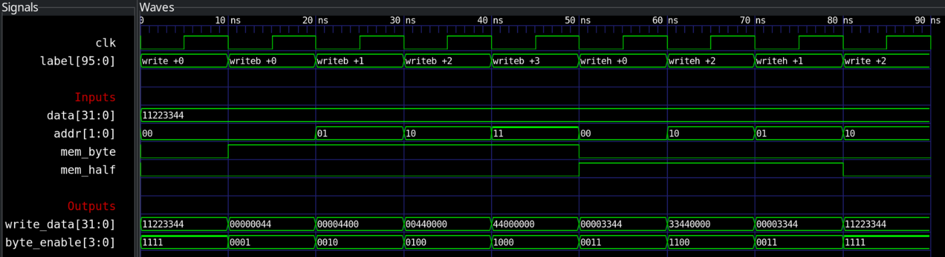
Here you can see the write alignment unit, writing 0x11223344 with every size at every place.
- The four
writebcases move the byte 44 through the word, and the byte enable moves along with it. - The last two cases are unaligned, and write at offset 0 instead.
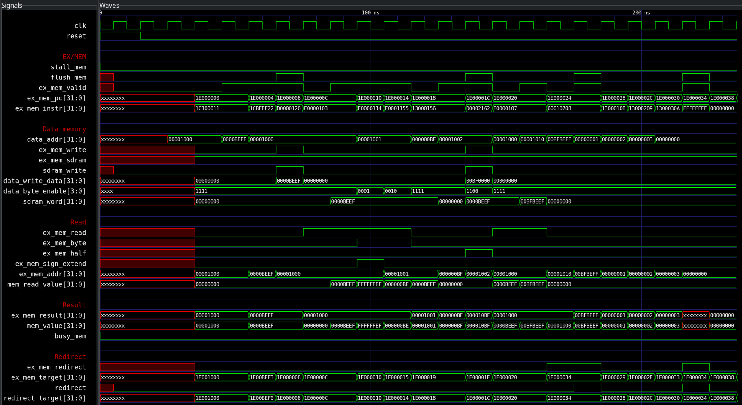
Finally, here you can see the demo program of MEM. It writes 0x0000BEEF, reads it back with three different sizes, and then writes a halfword over the upper half and reads the whole word again.
- During a write, the data address is the address of the write, and the memory write signal is 1 at the end of MEM. Otherwise, the data address is the address of the instruction in EX.
- After each write, the read behind it waits a cycle in EX, so there is a bubble in MEM.
- The
addafter thereadbuwaits a cycle in ID for the value it needs: the late-result stall. - The last read gives
0x00BFBEEF: the halfword write only changed the upper two bytes.
Next steps
The CPU can now read and write (simple) memory. Next up is the hardware stack for push and pop, together with the CPU-internal I/O registers, such as the stack pointer and the error register that reports things like unaligned accesses.