CPU part 4 - Register file
The register file, or sometimes called register bank or regbank, is the first component of the CPU that actually remembers something, so it is also the first one where the clock matters.
What the register file does
The register file holds the 16 registers r0 to r15, each 32 bits wide. Registers are the fastest storage in the CPU: almost every instruction reads one or two of them, and writes its result to one. Main memory is much slower, which is why efficient software tries to keep as much as possible in registers.
The register file has three ports:
- Two read ports, used in the ID stage. They get the register numbers
aregandbregfrom the decoder, and output the valuesareg_valueandbreg_value. Two ports, because an instruction likeadd r1 r2 r3needs both of its operands in the same cycle. - One write port, used by the WB stage at the end of the pipeline. When
writes_dregis set, the valuedreg_valueis written into registerdregat the rising edge of the clock.
Reading is combinational, like the ALU and the decoder: the value appears on the output as soon as the register number is there. Writing is synchronous: the register only changes at the clock edge. This combination is what makes it fit nicely in the pipeline: the ID stage reads the values during the cycle, and at the end of the cycle they are stored in the ID/EX pipeline register for the EX stage.
Design choices
Flip-flops instead of memory
An FPGA has blocks of RAM on the chip (on the Cyclone IV I use these are called M9K blocks), so you might expect the registers to go in there, and in many previous versions of the FPGC CPU they did. However, these RAM blocks can only be read with a clock edge in between: you give the address in one cycle, and get the data in the next. That would mean the register numbers would have to be known one stage earlier, before the instruction is even decoded. In a more textbook setting this is fine, because the registers become available at the start of the EX stage. That is what the previous version of the CPU (B32P3) did, but it needed quite some extra logic around the register bank to handle flushes and stalls, as those control logic signals are not included in the RAM itself. Because we only have 16 (technically 15) registers, I suspect this will be just fine timing and resource-wise, as they are just 15x32 flip-flops with two big multiplexers for the read ports. We will see! Worst case, I go back to my previous design for the register file in B32P3.
r0 is always zero
Why 15 and not 16 flip-flop registers? Because r0 is not stored at all: it always reads as 0, and writing to it does nothing. This is something the FPGC has always had (as do MIPS and RISC-V), and this is more useful than it sounds. A zero is needed all the time, for example to compare against in a branch, or to copy a register with or r1 r0 r2. Having it available for free also saves instructions. Writing to r0 is a convenient way to throw away a result, and nop is actually just or r0 r0 r0.
Write-through
There is one subtle case. Because the write happens in the WB stage at the end of the pipeline, an instruction in ID can read a register in exactly the same cycle in which an older instruction writes it. Without special care, it would read the old value, because the register only changes at the end of the cycle.
The solution is a so-called write-through (or write-before-read): when the register being read is the one being written in this cycle, the read port gives the new value dreg_value directly, instead of the old value from the flip-flops. This costs a compare and a multiplexer per read port, and saves us from handling this case somewhere else in the pipeline.
No stall logic inside
The register file has no stall, hold or clear inputs. If the ID stage has to wait, it simply reads the registers again in the next cycle, and thanks to the write-through it automatically sees anything that was written in the meantime. In B32P3 the register file had its own hold and clear logic, which was yet another place where the pipeline control was spread out over the design. Here, all of that stays in the pipeline registers themselves. Of course, the B32P4 design is still unproven at this point, but I am hopeful!
Simulation
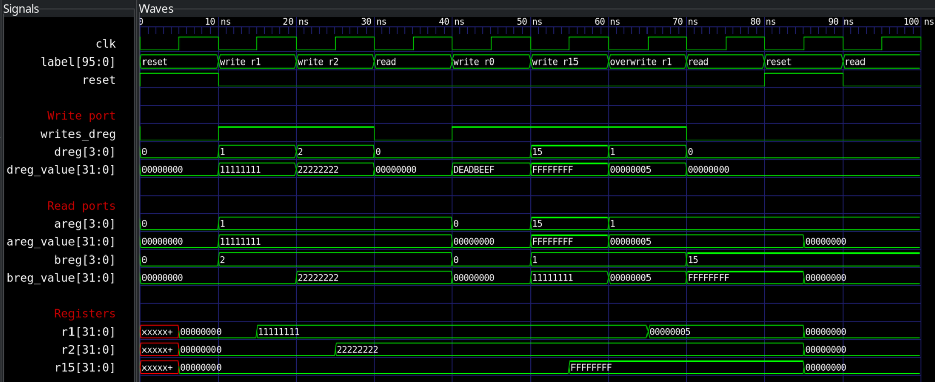
Here you can see the a simulation of the register file visualized in GTKWave. The values going in (write port) and coming out (read ports) change at the falling edges (note: in the actual cpu design everything happens at the rising edges), when the testbench applies the next case, while the registers themselves (r1, r2 and r15 at the bottom) only change at the rising edges. Some things to look at:
- Before the first reset, the registers are
x: unknown, shown in red. A flip-flop has no defined value until something is written to it, which is why the CPU needs a reset. I think that technically on an FPGA everything is initialized to 0 on boot, but still good practice to either include a reset at the start or initialize the registers explicitly in Verilog. - write r1:
areg_valuealready shows11111111during the whole cycle, whiler1itself only changes halfway, at the rising edge. That is the write-through in action. The same happens forr2on the B port one cycle later. - write r0: we write
DEADBEEFtor0, but readingr0still gives 0. - overwrite r1: both read ports read
r1while it is being written, and both get the new value 5. - reset: during the reset cycle the old values can still be read, and at the rising edge all registers become 0 at once.
Next steps
The register file always gives the values that have been written so far. But in a pipeline, the instruction directly ahead might still be busy computing the value we need, and will only write it a few cycles later. Detecting and solving that problem is the job of the hazard and forwarding units, which are next.