Introduction
Hi, as I am redesigning the FPGC project again, I want to take this opportunity to start creating a little blog series where I document the journey, challenges and thoughts building the FPGC. In this series I will go chronologically through the entire design, from CPU design and simulations all the way to high level software.
Part of the reason why I want to write a blog series is because this project has become huge, with many side tracks that did not end up in the current design, spanning multiple years of work. Over time, I start forgetting the details of certain parts, and writing a blog series will also help me in the future to go over this project again. It’s a bit like a journal.
In this first post, I will explicitly not go into the current technical state of the project. Instead, I will provide some background and history on the project, as an introduction to the first chapter of this series: the CPU design.
Background and History
The FPGC project started after a course on “Processors” in my Computer Science studies somewhere around 2018. The course was a basic introduction on how CPUs work, and at some point you had to design an extremely simple and basic CPU with logic gates in a very old and crappy Java program called Hades, and you had to write some assembly. While I had done a bunch of MCU programming before (mostly with Arduino), this course really started my interest in CPU design, as it taught me that CPU can be made relatively simple and understandable.
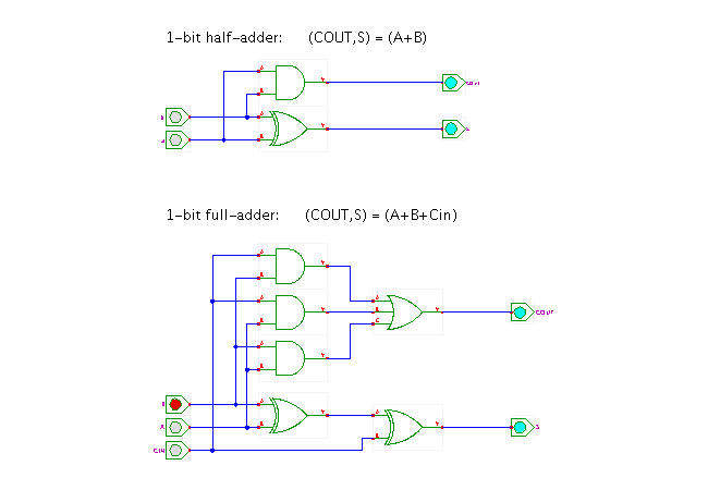
After completing the course, I was looking into ways to physically build something similar instead of using that Hades simulation program. My first intuition was to use logic gate ICs or even discrete components, but that quickly would become a hassle. At some point though, I came across FPGAs (Field-Programmable Gate Arrays), which almost seemed like the perfect solution. They looked like magic to me: a way to reprogram the logic on a big chip (which I later learned is due to programmable lookup tables and configurable interconnects). There were only a few remaining problems to solve before I could start getting into the world of FPGAs.
Verilog or VHDL?
When I started exploring how to actually use an FPGA, I quickly found out there were two main hardware description languages (HDLs, the language used to “program” FPGAs) commonly used: Verilog and VHDL. This was a tough decision as I could not find out which one was better or more popular at the time. Looking online, I found many debates and discussions, with one argument for Verilog that I still remember: apparently it resembles the C programming language more closely. Because I already had quite some C experience from working with microcontrollers, I decided to go with Verilog. Part of this was also because VHDL looked very verbose, and I do not like verbose languages in general. So Verilog it was.
FPGA development board, Altera or Xilinx?
When I started, I somehow had missed the part that you do not need physical hardware like an FPGA development board to start creating your first designs. There are simulation tools that allow you to start designing without needing to buy anything. I guess missing this made sense: microcontroller programming basically always require development boards to get started, and honestly the online tutorials were very limited at the time. I already knew at this point that the learning curve for FPGA development would be insanely steep, as basically nobody explained things in a beginner-friendly way. So I was looking for a development board to get me started, and again got at a decision crossroad: Altera or Xilinx? These two were clearly the main two brands at the time, and they clearly have their own completely proprietary ecosystems (which I still do no like as their software, and I tried both, are big bloated slow programs with license restrictions). They even have their own programmers, and everything was really expensive for a student without income. The choice was made easy: Altera has affordable knock-off “USB Blaster II” clones on AliExpress (and at the time Aliexpress was the only cheap way to get electronics), and the Xilinx programmers were >20 euro’s, which was above the amount you could buy without potential import fees. Also, there was a really nice and cheap (<20 euro’s) Cyclone IV EP4CE6 development board available there too, so I went with Altera.
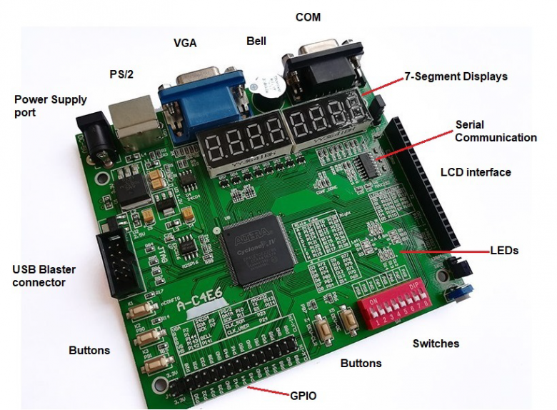
Another nice thing about this board is that there were quite some example designs included (mainly to test every feature of the board). This made it much easier to get started, as I could just modify existing designs to learn how things worked. I really liked that there was a VGA test pattern generator as well, which allowed me to create a small grid of colored squares that acted as visual output for my first programs. It was like I started with software programming all over again: modifying code examples and just try thing until they work. Over the next few months, I was able to do some cool first projects, like reading GameBoy display outputs via the gpio pin row, and displaying them over VGA using a small internal SRAM buffer.
The start of FPGC
Once I got a bit comfortable with the basics (which interstingly still did not include simulation), I started to try creating something that resembles a CPU, which I would program by manually writing ones and zeroes in a memory initialization file. This all was not working too great, but I remember being able to get a snake program working on a modified VGA test-pattern generator output. I already started to call that project FPGC, which was then more game focussed and stood for “FPGA Game Console”, since I was able to get a NES controller connected and wanted to create my own games. After a lot of experimentation with FPGC1 and FPGC2, I wanted to restart again with my new experiences and knowledge. At this point I learned more about simulation and came across the best piece of FPGA software: Icarus Verilog together with GTKWave for waveform visualization. These two pieces of software were so much easier to understand than the included simulator in Altera’s Quartus Prime, that they allowed me to actually see under the hood what was happening in my designs, not having to rely on 7-segment display or VGA output anymore. Furthermore, these tools are really lightweight, allowing me to quickly iterate. At this point I was able to actually design a proper CPU with a fetch, decode, execute, memory and write-back stage. To me, this is the moment when the project really started to take shape. During FPGC3 I also started to understand the clock domain crossing problem better, which had plagued the project many times before, and was especially frustrating because it caused the hardware not to act like the simulations. At this point, I was able to build a little computer, moved over to a Cyclone EP4CE15 development board with plenty of IO pins, and restarted the project quite some times to rebuild with better architecture using the learnings from the previous iterations. After FPGC4, FPGC5, and FPGC6, we arrive at FPGC, which is meant to be the 1.0 version the project. I was able to achieve basically all of my project goals with this iteration, but at some point the project became a big mess due to growth of the project. The rewrite I am now starting with will make me get familiar with the core components again, and allows me to rewrite them in a clean way, knowing how the end state looks like.
Next Steps
Now I wrote down how the project evolved to where it is now, we can start with the actual FPGC design. The next blog posts will go into the CPU design.