SoC part 1 - Device bridge and the first IO devices
The CPU is done for now, so it is time to build the system around it so we can get the CPU running on a real FPGA with a minimal design containing ROM for a test program, SDRAM for main memory, and UART to talk to the PC. Let’s make this a new series of posts called “SoC”, which is everything around the CPU. In this first post, I (re)define the memory map, connect the first devices to the CPU over the bus using a new module called the device bridge, and build the first simple devices: a cycle counter, timer, and a register for the LED and DIP switches on the PCB. UART gets its own post as it is more complex and this post will already be quite long.
Cleaning up the memory map
In the post about memory, I kept the memory map of the previous FPGC design as it was. Before I start writing a lot of software against it, this is the moment to improve it because every program will depend on it.
The old memory map grew over many versions of the FPGC. For example, the large gap between SDRAM and the I/O region at 0x1C000000 was made for the large DDR3 memory on a Xilinx board that I used for a while, and dropped later. The VRAM regions were placed wherever there was room at the time. None of that has a reason anymore, and since I already made my custom PCB I know the sizes of the memories and which IO devices will need to be connected. So here is a better fitting layout:
| Address | Size | What |
|---|---|---|
0x00000000 | 64 MiB | SDRAM |
0x04000000 | 16 MiB region | boot ROM, 4 KiB for now |
0x05000000 | 16 MiB region | GPU’s memories (later) |
0x06000000 | 16 MiB region | external SRAM (later) |
0xFFFF8000 | 32 KiB | device registers, 256 bytes per device |
0xFFFFFF00 | 256 bytes | CPU-internal registers |
Some notes:
- All memories are below 128 MiB, which is the range of the absolute
jumpinstruction. This way, code in SDRAM can jump straight to ROM (if I ever need to do so). - The GPU and external SRAM (which will be used for the GPU framebuffer) get a region of 16 MiB each. The GPU is not redesigned yet (I have some cool plans for that), but this leaves it plenty of room.
- There is no region for flash or the SD card. These memories will be accessed through SPI controllers in software rather than being memory-mapped. This has both advantages and disadvantages in terms of speed and complexity, but given the huge amount of SDRAM available, this is an acceptable trade-off for me as I can use caching in software instead.
Every device register in one instruction
The most interesting choice is putting the device registers at the very end of the address space. That looks strange at first, but it saves an instruction for every access to a device.
A read or write adds a 16-bit constant to a register to get the address. That constant is sign-extended: if its highest bit is 1, it is a negative number, and the upper 16 bits of the address become 1 as well. With r0, which is always 0, as the register:
| Constant (16 bits) | As a number | Address |
|---|---|---|
0x0010 | 16 | 0x00000010 |
0x7FFC | 32764 | 0x00007FFC |
0x8000 | -32768 | 0xFFFF8000 |
0x8104 | -32508 | 0xFFFF8104 |
0xFFFC | -4 | 0xFFFFFFFC |
So with r0 and a negative constant, a single instruction reaches any address in the last 32 KiB, which is exactly where the device registers and the CPU-internal registers are. Since I have full control over the assembler too (at some point I should write a small series too on the build toolchain), I made it accept the full address directly and let it convert it to the appropriate constant automatically. For example:
write 0xFFFF8000 r0 r1 ; the same as write -32768 r0 r1With the old I/O region at 0x1C000000, a program first had to put the address in a register, which takes two instructions, or keep it in a register all the time. Every device access in a driver now saves that.
Each device gets 256 bytes of its own, which is room for 64 registers. No device needs that many, but it keeps the registers of a device together, and a device can get more registers later without moving the next one. To visualize:
0xFFFF8204 = 1111 1111 1111 1111 1 | 000 0010 | 0000 0100
             all ones              | device 2 | register 4
             "a device register"   | (timer)  | (control)
A bridge to the devices
The CPU only knows about four kinds of addresses: SDRAM, ROM (for fetching instructions), its own internal registers, and everything else. Everything else goes over the bus from the last CPU post. Something has to sit at the other end of that bus and know which device is at which address.
Old PCs had a nice name for this. The CPU was connected to a chip called the northbridge, which handled the fast things: memory and graphics. The northbridge connected to the southbridge, which handled all the slow things, and had many of them inside: timers, interrupt controller, serial ports, connections to keyboard/mouse, and storage. They were called north and south because of where they were placed on the motherboard, with the CPU at the top.
The FPGC has a similar split. The fast path is the caches, which talk to the SDRAM controller directly. The slow path is the bus, which ends at what I call the device bridge. It is not really south of anything, but if it was then southbridge would be a fitting name.
In the previous FPGC versions, this was the Memory Unit: one module that knew the address of every register, and had the devices inside (initially also the SDRAM, hence Memory Unit, but at some point this became just I/O and slower memories). I liked that you could read one module and see everything that happens on every access, so the device bridge works the same way. The difference is in how the work is split:
- The bridge knows the address of every register, and answers every access. It does not know how any device works.
- Each device is its own module, which only does its own job. It does not know anything about the bus or about addresses.
                   +----------------------------------------------+
 CPU bus <-------> | device bridge                                |
                   |                                              |
 ROM <-----------> |   +------+ +---------+ +-------+ +-------+   |
                   |   | UART | | cycle   | | timer | | board |   |
                   |   |      | | counter | |       | |       |   |
                   |   +------+ +---------+ +-------+ +-------+   |
                   +------|---------------------|---------|-------+
                          |                     |         |
                       rx, tx              interrupt    LED, switches
How the bridge answers
The heart of the bridge is a list with every register. For each register, it says what a write does and what a read gives. For the timer, that looks like this:
| Address | Register | A write | A read |
|---|---|---|---|
0xFFFF8200 | COUNT | tells the timer to start counting down from the written value | the timer’s count |
0xFFFF8204 | CONTROL | tells the timer its new settings | the timer’s settings |
0xFFFF8208 | STATUS | tells the timer to clear its flag | the timer’s flag |
An address that is not in the list gets an error as its answer, and so does a device register that is not accessed as a whole word. The CPU then sets the bad-address flag of its error register. This way, a wrong pointer does not go unnoticed, and the CPU never waits forever for an answer that nobody gives.
The bridge answers from its own registers, in the cycle after the request. Reading the timer’s control register goes like this:
| Cycle | What happens |
|---|---|
| 1 | the CPU sends the request. The bridge finds the address in its list, and takes the timer’s settings. |
| 2 | the bridge answers with “ready” and the settings |
A write works the same way, but the bridge also tells the device what to do, at the same time as its answer to the CPU:
| Cycle | What happens |
|---|---|
| 1 | the CPU sends a write of 1000 to COUNT |
| 2 | the bridge answers with “ready”, and tells the timer to start from 1000 |
| 3 | the timer counts 1000 |
Doing everything from registers costs a cycle here and there, but it keeps every path in the bridge short: from a register, through a bit of logic, into the next register. The devices are slow anyway compared to the CPU, so a cycle more does not matter. I care more about having the entire design pass timings at 100 MHz.
A lot of accesses will not be answered right away, especially when I start adding more external devices instead of internal registers. Currently there are already a few:
- A read of data from the ROM. The ROM is a block RAM, which gives its word a cycle after it gets the address, so the bridge waits a cycle.
- A read of a byte that the UART received. The bridge first tells the UART to take the byte from its buffer, and then waits for it.
- A write to the UART when its buffer is full. The bridge waits until there is room.
For these, the bridge only has to remember that it is waiting. The bus keeps the address the same until the answer, so in every cycle, the bridge just looks at the address again, and answers once it can.
Devices with their own ports
Because the bridge does all the talking to the CPU, a device only gets what it needs to do its job. The timer, for example, gets these from the bridge:
- start counting down, and the count to start from
- new settings: whether to repeat, and whether to interrupt
- clear the flag
And it gives back its count, its settings, its flag and its interrupt. The timer does not know that its settings are in bit 0 and bit 1 of a register at 0xFFFF8204. Only the bridge knows that. So when I want to move a register or change its bits, I only change the bridge, and when I want to change how the timer counts, I only change the timer. I like this separation of concerns.
One way to interrupt
Some devices need to get the attention of the CPU: the timer when it expires, and UART when a byte arrives. Later there will be more, including external chips on the board like the CH376 for USB and the ENC28J60 for Ethernet. I wanted one rule that works for all of them, internal and external:
- A device has a flag in its status register that says something happened.
- It has an enable bit in its control register, which is 0 after a reset.
- Its interrupt output is “the flag and the enable bit”, a level that stays 1 as long as both are 1.
- The CPU makes the interrupt pending when that level goes from 0 to 1.
- The interrupt handler clears the cause, for example by writing the timer’s status register, or by reading the UART until no byte is waiting.
Here is how that plays out for the timer:
| What happens | Flag | Enable | Output | CPU |
|---|---|---|---|---|
| the timer expires, with the interrupt disabled | 1 | 0 | 0 | nothing |
| the program enables the interrupt | 1 | 1 | 1 | the output rises: interrupt |
| the handler clears the flag | 0 | 1 | 0 | |
| the timer expires again | 1 | 1 | 1 | the output rises: interrupt |
The reason for a level instead of a short pulse per event is the external chips. Their interrupt pins are levels that stay active until the cause is cleared over SPI, so a level fits them exactly. Their pins do not go to the CPU directly though: they go into the status register of the FPGA module that talks to the chip, with the same kind of enable bit. That way, every interrupt in the system works the same, whether it comes from inside the FPGA or from a chip on the board.
The first devices
With the bridge in place, these are the first three devices. They are small, but are useful to measure, wait, and see what is going on when I bring the design up on real hardware.
The cycle counter
A 64-bit counter that counts every clock cycle since the reset, for measuring how long code takes. At 100 MHz, it takes more than 5,000 years to wrap around, so it never does in practice. A timer could also be used for this, but is less precise, especially since interrupts are only taken in instructions that redirect the program counter.
The CPU is 32 bits, so a program reads the count in two halves. If it read the running counter directly, things go wrong at the moment the low half wraps around. Say the count is 0x00000000_FFFFFFFF when the program reads the low half, and 0x00000001_00000000 when it reads the high half one cycle later. The program then gets 0x00000001_FFFFFFFF, which is more than 4 billion cycles too far.
So the counter has a snapshot instead:
| Address | Register | A write | A read |
|---|---|---|---|
0xFFFF8100 | SNAPSHOT | copies the whole count into the snapshot | 0 |
0xFFFF8104 | LOW | the low half of the snapshot | |
0xFFFF8108 | HIGH | the high half of the snapshot |
A write copies the whole count at once, and the snapshot does not change until the next write. The program can then read the two halves in any order, as often as it likes, and they always belong together.
Measuring a piece of code is then: take a snapshot and read its low half, run the code, and do the same again. The difference is the number of cycles. Taking a snapshot and reading it takes a few cycles itself, so measuring nothing at all gives a small difference too, which you subtract once. For anything shorter than 42 seconds, the low halves alone are enough.
The previous FPGC had a counter of microseconds instead. Counting cycles is simpler, as it needs no divider for the clock, and it is more precise, which is exactly what you want when you measure code. While very small pieces of code can be measured using simulation, anything slightly complex or requiring external devices needs to be measured on real hardware, and this counter allows for precise measurements there.
The timer
The timer counts down by one every cycle, and sets its flag when it reaches 0. Timers are useful for many different things, such as implementing a wait/sleep/delay function, generating periodic interrupts for repeating tasks, or keeping track of elapsed time (although FPGC now has a cycle counter, so this is less necessary).
| Address | Register | A write | A read |
|---|---|---|---|
0xFFFF8200 | COUNT | starts counting down from this value. 0 stops the timer. | the cycles left |
0xFFFF8204 | CONTROL | bit 0: repeat. Bit 1: interrupt. | the same bits |
0xFFFF8208 | STATUS | clears the flag | bit 0: the flag |
It has two modes. In one-shot mode, it stops at 0. In periodic mode, it starts again from the same value right away. With a count of 4, periodic, the count goes like this:
| Cycle | 1 | 2 | 3 | 4 | 5 | 6 | 7 | 8 | 9 |
|---|---|---|---|---|---|---|---|---|---|
| Count | 4 | 3 | 2 | 1 | 4 | 3 | 2 | 1 | 4 |
| Flag set | yes | yes |
Periodic mode is meant for a steady tick, such as the scheduler of an OS later. It could also be done in one-shot mode, with the interrupt handler starting the timer again. But the handler only gets there some time after the timer expired: the CPU first has to finish what it is doing, jump to the handler, and save some registers. Say the tick should be every 1,000 cycles, and the handler always needs 50 cycles before it starts the timer again. Then every tick is 1,050 cycles apart, and after 100 ticks, the clock of the OS is 5,000 cycles behind. In periodic mode, the timer starts again in the same cycle that it expires, so it never drifts, no matter how long the handler takes.
Another common way to make a timer is a compare register next to the cycle counter, like RISC-V does: the interrupt comes when the counter reaches the value in the compare register. That gives one time base for everything, but it needs a 64-bit compare register that is written in two halves, which has the same problem as reading the counter in two halves. A countdown in 32 bits is simpler, and still goes up to almost 43 seconds.
The previous FPGC had three timers, which counted in milliseconds. For now, I start with one, and add more when needed. In the future, if I ever need to wait for longer than 43 seconds, I might extend the control register to allow for a multiplier to the number of cycles per tick to allow for longer delays.
The board register
The PCB I made for the FPGC (I am just going to call that “the board”) has nine LEDs at the front and four DIP switches. They do not really belong to a specific device, so I expose them through a simple board register. However, most of the LEDs are activity leds and should not be controlled from software directly, as they are meant to reflect the activity of other devices rather than be manually toggled by the CPU. I will talk more about the LEDs when I create a blog post on the PCB, but for now, there is one LED labeled “User” that should be controlled by software.
| Address | Register | A write | A read |
|---|---|---|---|
0xFFFF8300 | LED | bit 0 turns LED “User” on or off | the LED state |
0xFFFF8304 | SWITCHES | the four DIP switch states |
There is one interesting detail in reading the switches. A switch can change at any moment, not in step with the clock of the FPGA. If it changes just as a flip-flop samples it, the flip-flop can end up in between 0 and 1 for a short while, before it falls to one side. This is called metastability. If that undecided value goes straight into the logic behind it, one part of the design could see a 0 and another part a 1. The usual fix is a synchronizer: two flip-flops in a row. The first one may become undecided, but it has a whole cycle to settle before the second one samples it, so the rest of the design only sees a clean 0 or 1. A change of a switch then shows up in the register two cycles later, which is unnoticeable for human input. Note that these stabilizers are needed for all asynchronous inputs to the FPGA.
Simulation
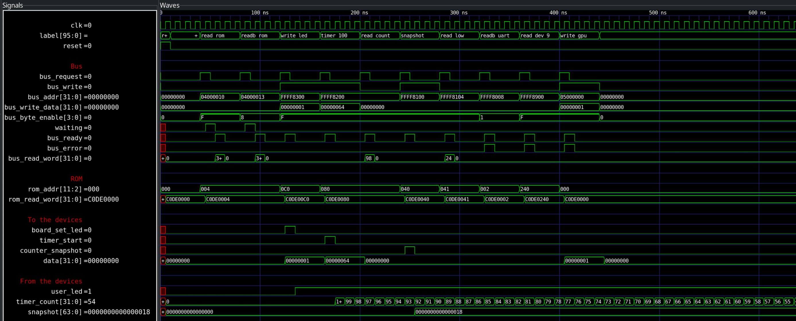
Here you can see the device bridge, with its devices inside, and a ROM that the testbench plays.
- First a word and a byte are read from the ROM. The bridge waits a cycle for the ROM’s word, and answers in the cycle after.
- Then a write to the LED and a write to the timer’s COUNT. The bridge answers in the next cycle, and at the same time tells the device what to do. The LED and the count change a cycle later.
- The read of the count gives what is left of it, and the snapshot of the cycle counter is taken in the same way.
- The last three accesses go nowhere: a byte read of a device register, device 9, which does not exist, and the GPU’s region, which is empty for now. The bridge answers each of them with an error.
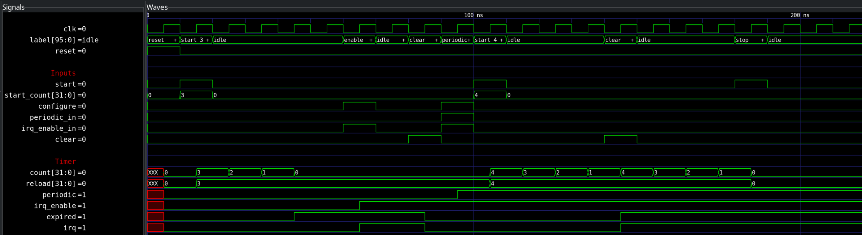
Here you can see the timer on its own, which follows the table from the interrupt section above.
- The timer counts down from 3 with its interrupt disabled. It expires, and only its flag goes up.
- When it gets the setting to interrupt, the output rises right away, and stays up until the flag is cleared.
- Then it runs periodically every 4 cycles: the count starts again by itself every time it reaches 0, until it is started with a count of 0, which stops it.
Next steps
To get a first hardware test running, there are a few final things left: UART, and the top-level design for the FPGA. The next post will cover either or both of these topics.